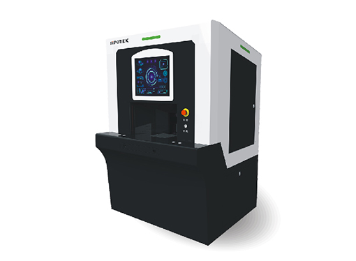
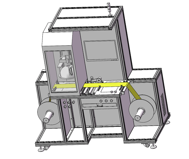
[Application Case] PCB appearance visual inspection equipment
PCB appearance visual inspection is the process of using visual technology to detect and evaluate the appearance quality of PCB board.
Equipment characteristics
High-precision detection: Through high-resolution image acquisition equipment and precision algorithms, it can achieve accurate detection of PCB appearance defects, welding quality, component location, etc.
Automated inspection: PCB appearance inspection can be carried out with automated equipment to improve inspection efficiency, accuracy and consistency.
Versatility: Supports the detection of various appearance characteristics of the PCB board, such as defects, defects, printing quality, etc.
Fast feedback: can generate real-time inspection report and result feedback, help production personnel to adjust the production process in time.
Data management: Support the recording, analysis and management of test data to support quality control and production optimization.
Application field
Electronic manufacturing: Used for PCB appearance defect detection, welding quality detection, component location detection, etc.
Communication industry: Used in communication equipment PCB appearance quality inspection to ensure equipment reliability.
Automotive electronics: Used to detect the appearance of the PCB board in the automotive electronics module to ensure the normal operation of the automotive electronics system.
Industrial control: Used in industrial control equipment PCB appearance quality inspection to ensure equipment stability.
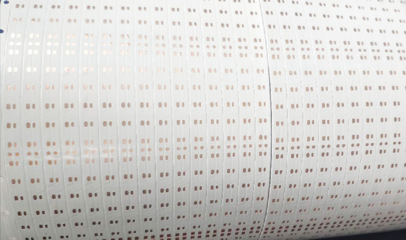
Detected object
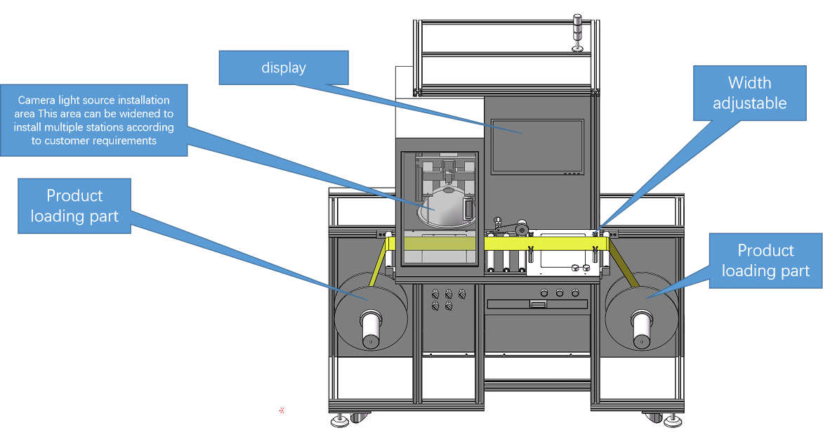
Equipment inspection
【 Detection effect 】
Top positive lighting effect: Detection items: bare copper, whether there is copper in the hole
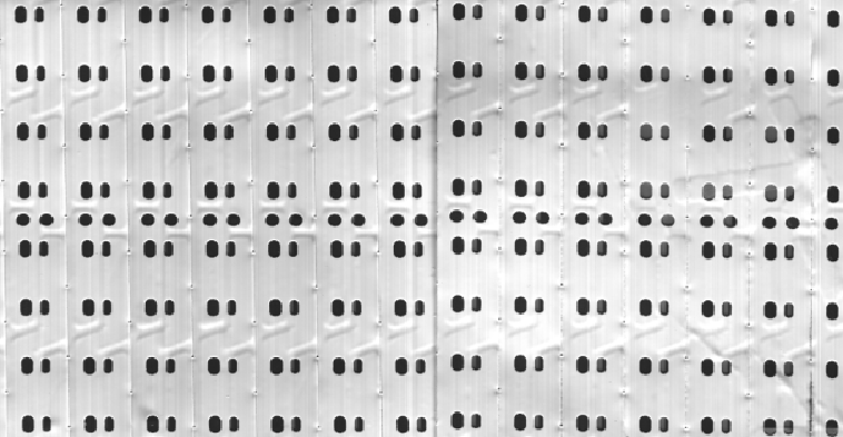
Bottom positive lighting effect: Detection items: distinguish empty, single layer, double layer copper
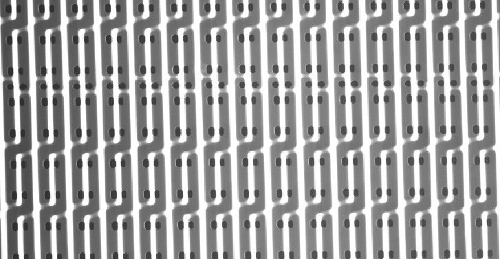
-
Service hotline
13077808017

